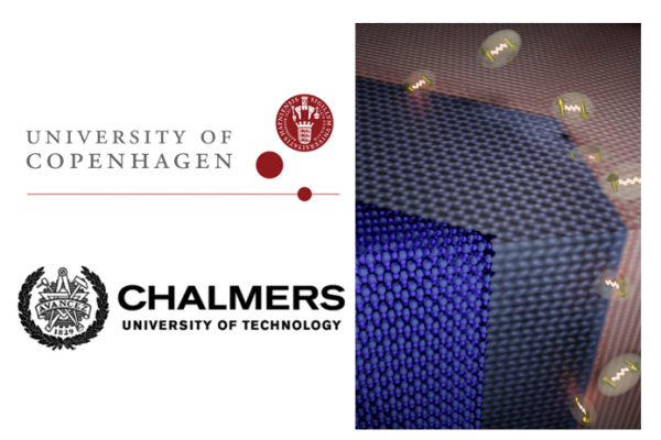
TA Success Stories: Superconducting Pb on semiconducting InAs nanowires, from the University of Copenhagen to CMAL Gothenburg

Many successful projects stem from transnational access provided by ESTEEM3. This week, we focus on the “Superconducting Pb on semiconducting InAs nanowires” project from University of Copenhagen (Denmark) which was granted access to the Department of Physics at Chalmers University of Technology in Gothenburg (Sweden) one of the ESTEEM3 TA provider.
The “Superconducting Pb on semiconducting InAs nanowires” project, carried by Dr. Thomas Kanne from the University of Copenhagen (Denmark), was granted access to facilities and expertise of the Department of Physics at Chalmers University of Technology in Gothenburg (Sweden)in Summer 2019, as part of the transnational access activities of ESTEEM3.
Introduction
Within condensed matter physics, epitaxial semiconductor-superconductor materials are currently investigated for their ability to host novel quantum states and in these efforts, their candidacy as model systems for next generation quantum hardware are assessed. Depending on their interface integrity, these heterostructures may act effectively as a hybrid between the semiconductor and the superconductor. Here, the underlying material can exhibit engineered material specific properties such as induced superconductivity.
Thanks to ESTEEM3 TA, key structural parameters of a new material combination utilizing Pb as the superconductor could be correlated to sub-kelvin electron-transport experiments.
The main results of the project
By use of high-resolution high angle annular dark field scanning transmission electron microscopy a particular small bi-crystal interface domain match between InAs and Pb was revealed. With the atomic resolution of this technique, the interface along different crystallographic directions was found to be abrupt and the Pb films contained no grain boundaries along the long axis of the nanostructures. Advanced focus ion beam was used to fabricate cross-sections of the nanostructures, uncovering the single crystalline nature of the Pb films. These observations are central for the quantum-transport community, as the single crystal nature, for instance, indicate suppressed potential for impurity-generated discontinuities of the hybrid wavefunction.
Detailed understanding of the specific materials, and in particular their interfaces, is of outmost importance for the continued progress in the field of hybrid materials and the potential realization of topologically protected qubits.
Successful outcomes
Dr. Thomas Kanne published one article in a renownedjournal:
- Nature Nanotechnology 2021 (https://doi.org/10.1038/s41565-021-00900-9)
Interested in Transnational Access to the leading European state-of-the-art Transmission Electron Microscopy (TEM)? Find out more about the procedure here!
