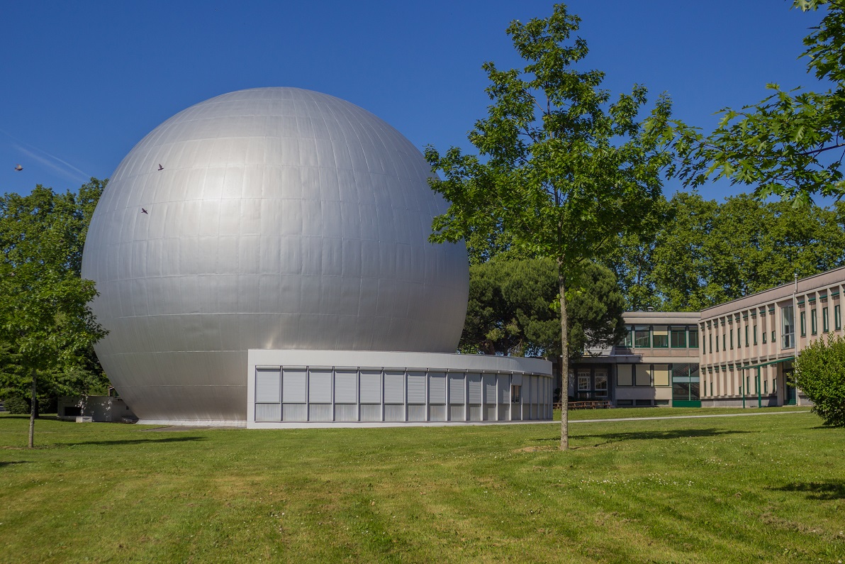
CEMES is a laboratory for fundamental research in materials science, solid state physics, and molecular chemistry. The scientific activities developed at Cemes cover the synthesis of (nano) materials and molecular systems, as well as the study and modeling of their structure and physical properties. The TEM infrastructure at Cemes is part of an extensive range of instruments used to characterize the properties of materials and molecules at the nanometer or atomic level.

For TEM sample preparation, the CEMES is equipped with a state-of-the-art Focused Ion Beam (FIB) Helios-NanoLab 600 from FEI. This FIB is fitted with 5 GIS (Gas Injection System) with tungsten, platinum, cobalt, oxygen and carbon sources, an Omniprobe System for easily manipulating TEM lamellae during the thinning process, and EBSD (Electron Back-Scattered Diffraction) and EDS detectors. Beside this FIB, the usual techniques for sample preparation are available at CEMES including saws and ultra-sonic grinders, two tripod polishers, two Precision Ion Polishing Systems (PIPS) equipped with CCD cameras, chemical polishing and electro polishing facilities.
(i) The unique Hitachi HF3300-C, Cs corrected (B-Corr) dedicated for electron holography and in-situ TEM (I2TEM). This 300 kV TEM has been specially designed to perform electron holography and in-situ experiments at the highest level. It is fitted with a cold field emission gun (C-FEG) and is equipped with a spherical aberration corrector (“Aplanator” B-corr). I2TEM is also fitted with the latest generation of energy filter GIF Quantum ER-965 for spectroscopy applications, four rotatable electrostatic biprisms for advanced electron holography and interferometry experiments and a fast 4Kx4K OneView camera (Gatan) essential for in-situ experiments. Two goniometers allow working either in conventional HREM mode (with ultimate spatial resolution up to 80 pm) or in field-free environment (Lorentz mode) with 0.5 nm ultimate resolution.
The I2TEM is fitted with many stages for in-situ experiments i.e. single, double tilt, tilt-rot stages, heating / cooling stage with 4 electric contacts for in-situ biaising, nano-indentor (Hysitron), magnetizing stage (Hummingbird).
(ii) The imaging Cs-aberration corrected FEI-Tecnai F20 (SACTEM): This microscope is fitted with a Schottky field emission gun and an imaging Cs aberration corrector offering 120 pm resolution. An energy filter, 863 GIF Tridiem, enables image filtering and EELS. A scanning set up and dark-field detectors have been added for STEM experiments. Off-axiselectron holography experiments can be performed using a rotatable electrostatic biprism. Besides the usual single and sample holders, a unique “nano-indentor/STM” double-tilt stage from Nanofactory is available for SACTEM allowing local straining or local electrical contacting measurements.
(iii) The JEOL 2010-HC dedicated in-situ straining TEM. The JEM2010-HC is a 200 kV TEM suited for in-situ experiments using dedicated specimen holders. It is fitted with a Mega-View III camera enabling video sequences to be recorded. There is also a unique collection of specimen holders (double tilt, straining holder, heating/straining holder) available for in-situ experiments.
CEMES scientists operate sophisticated commercial and home-made software, as well as a data analysis infrastructure to derive optimal research output including several codes for electron holography analysis (for magnetic, electrostatic and strain quantitative data), strain analysis software (GPA) for high resolution images. Several software packages and scripts for general data processing software are developed in house, provided to external users and offered within transnational access.
- How Transnational Access works?
- Request for access
-
Installations
- Access to StEM Stuttgart
- Access to ERC Juelich
- Access to CEMES Toulouse
- Access to LPS Orsay
- Access to EMAT Antwerp
- Access to OXTEM Oxford
- Access to WEMS Cambridge
- Access to K7 Ljubljana
- Access to FELMI-ZFE Graz
- Access to LMA Zaragoza
- Access to Advanced DME Cadiz
- Access to IC-EM Krakow
- Access to CMAL Chalmers
- Access to Gemini Centre Trondheim
- Access to Beyondnano EM lab Catania
