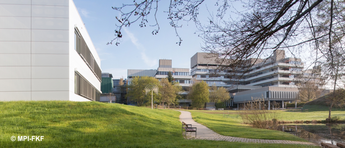
The Stuttgart Center for Electron Microscopy (StEM) is hosted at the campus of the Max Planck Institute (MPI) for Solid State Research and the MPI for Intelligent Systems. Both institutes cover a wide range of scientific activities aimed at manufacturing, understanding, modelling, and manipulating matter at length scales from the micrometre range down to the atomic level. The StEM possesses outstanding expertise in electron microscopy techniques and development.

A dual-beam Focused Ion Beam (FIB) FEI Scios equipped with a Gas Injection System (GIS) containing a Pt and a C source, an EasyLift EX NanoManipulator for in-situ micro-manipulation of the specimen and TEM lamella transfer, an EDAX EDX-EBSD TEAM Pegasus System and an Oxford Instruments EBIC E3 Electrical Microanalysis System. A Fischione Nanomill and conventional sample preparation facilities including several Gatan Precision Ion Polishing Systems, a Fischione plasma cleaner, a Leica C/Au/Ir sputter coater, Buehler diamond wire saws, ultra-sonic grinders, Allied MultiPrep System TEM wedge polishers, Struers Tenupol electrolytic polishers, and Leica (Cryo-)Ultramicrotomes.
The comprehensive suite of electron microscopy tools built up by StEM is unique by world standards. Both TEMs are of the latest generation operating at voltages of 30 kV, 60 kV, 80 kV and 200 kV, equipped with a cold field-emission gun, a Gatan GIF Quantum ER(S) energy filter with DualEELS and FastEELS options, a Centurio energy-dispersive X-ray system with a large solid angle SDD X-ray detector, Gatan UltraScan 1000XP and Gatan Orius SC200D CCD cameras, a Quantum Detector Merlin direct electron detector as well as with HAADF, ABF, and BF detectors, having high energy resolution at high spatial resolution. In STEM mode, the ARM200F allows imaging at a spatial resolution of 61 pm at 200 kV and of 136 pm at 30 kV, and in HRTEM mode it exhibits an information limit of 71 pm at 200 kV and of 134 pm at 30 kV. For both TEMs special sample holders are available for in-situ heating and cooling, in-situ heating and biasing with 8 probes, double tilt tomography, and 360°-tilt-tomography for needle-shaped specimen.
StEM operates sophisticated software and a data analysis infrastructure to derive optimal research output including a suite of microscopy simulation packages to quantitatively interpret electron diffraction data, high resolution images, and electron energy-loss spectra, and to build 3D structural models. Several software packages and scripts for general data processing software in Digital Micrograph and Matlab are routinely developed in house, provided to external users and offered within TA. The data analysis is offered together with and provided under the installation TEM.
StEM’s investigators, consisting of 3 senior scientists, 5 postdoctoral students, 6 PhD students and 9 technicians and engineers, include experimentalists and theorists, physicists and chemists, with individual expertise in many different areas, including interfaces, mechanical properties, strained semi-conductors, complex oxides, semiconducting and metallic nanostructured thin films, nanoparticles, and heterostructures. These world leading scientists sustain outstanding expertise in advanced electron microscopy techniques which are offered to transnational access users.
- How Transnational Access works?
- Request for access
-
Installations
- Access to StEM Stuttgart
- Access to ERC Juelich
- Access to CEMES Toulouse
- Access to LPS Orsay
- Access to EMAT Antwerp
- Access to OXTEM Oxford
- Access to WEMS Cambridge
- Access to K7 Ljubljana
- Access to FELMI-ZFE Graz
- Access to LMA Zaragoza
- Access to Advanced DME Cadiz
- Access to IC-EM Krakow
- Access to CMAL Chalmers
- Access to Gemini Centre Trondheim
- Access to Beyondnano EM lab Catania
